- [[#introduction|introduction]]
- [[#sign secure boot|sign secure boot]]
- [[#KEK and DKEY|KEK and DKEY]]
- [[#KEK and DKEY#如何使用DKEK (了解)|如何使用DKEK (了解)]]
- [[#OTP|OTP]]
- [[#keyWriter|keyWriter]]
main domain
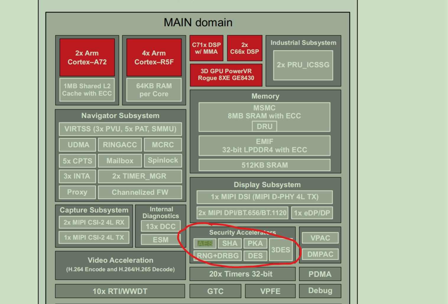
加密硬件加速器 – 带 ECC 的 PKA、AES、SHA、 RNG、DES 和 3DES
Asymmetrische Kryptografie: RSA und ECC-Funktionen
• Hash-Funktionen: Message Digest Algorithm (MD5), SHA1 und SHA2-224/256/384/512
• Symmetrische Kryptografie-Funktionen: AES-128/192/256
• Hardware-TRNG-Modul mit Nachbearbeitung für einen deterministischen Zufallsbitgenerator (DRBG)
wakeup domain DMSC

Main components of the DMSC are:
•Arm Cortex-M3 processor core (ARMv7-M architecture profile)
•160 KB ROM to allow boot sequence, authentication and provide security service (M3 accessible only)
- Two separate local memory banks for Instruction code (I-code) and Data space (D-code) with single error correction and double error detection
- Firewall enabled 32-bit VBUSP CBASS interconnect
- Interrupt Aggregator with support of up to 80 interrupt inputs to the DMSC
- Four dual-mode 32-bit timers
- DMSC control module - contains various control, configuration and status MMRs for power management functions
- Security Manager module for device security management, device type control (GP, EMU, HS), emulation and JTAG control, and key management
- AES engine with 128, 192 and 256-bits support and DPA/EMA countermeasures
TIFS world 安全通信能力
SoC中的每个物理处理器都有能力在不同的模式下运行,如特权和非特权,安全或不安全。主机的定义超出了物理处理器的范围,也区分了处理器的操作模式。
On devices with distributed TIFS and DM services across multiple cores, the interaction between the hosts and the security and device manager is as below:

Software on different cores and secure proxy communication channels
For secure cores the communication mechanism is as below:
这一层通过了DMSC的加密中转, 为了开发一种安全的车辆 E/E 架构,需要在 ECU 内部实现一套复杂的加密计算过程。TI 为了解决这个问题,在 DMSC 中集成了AES,RNG,SHA 等安全加速器,用来对启动过程中的加密,验签提供硬件加速,这些硬件 IP 对上层提供的服务可以通过标准的 crypto driver 被调用
For messages running from MCU R5F the communication mechanism is as below:
For messages running from other non-secure cores the communication mechanism is as below:
secure Proxy J7 描述
J721E Secure Proxy Descriptions
Secure Proxy thread allocation for NAVSS0_SEC_PROXY_0
| Secure Proxy Thread ID | Direction (write or read) | Number of Messages | Host | Host Function | IRQ (threshold) | IRQ (error) |
|---|---|---|---|---|---|---|
| 0 | read | 2 | A72_0 | notify | COMPUTE_CLUSTER0_CLEC/SOC_EVENTS_IN_64, COMPUTE_CLUSTER0_GIC500SS/SPI_64 | COMPUTE_CLUSTER0_CLEC/SOC_EVENTS_IN_64, COMPUTE_CLUSTER0_GIC500SS/SPI_64 |
| 1 | read | 30 | A72_0 | response | COMPUTE_CLUSTER0_CLEC/SOC_EVENTS_IN_65, COMPUTE_CLUSTER0_GIC500SS/SPI_65 | COMPUTE_CLUSTER0_CLEC/SOC_EVENTS_IN_65, COMPUTE_CLUSTER0_GIC500SS/SPI_65 |
| 2 | write | 10 | A72_0 | high_priority | N/A | N/A |
| 3 | write | 20 | A72_0 | low_priority | N/A | N/A |
| 4 | write | 2 | A72_0 | notify_resp | N/A | N/A |
| 5 | read | 2 | A72_1 | notify | COMPUTE_CLUSTER0_CLEC/SOC_EVENTS_IN_66, COMPUTE_CLUSTER0_GIC500SS/SPI_66 | COMPUTE_CLUSTER0_CLEC/SOC_EVENTS_IN_66, COMPUTE_CLUSTER0_GIC500SS/SPI_66 |
| 6 | read | 30 | A72_1 | response | COMPUTE_CLUSTER0_CLEC/SOC_EVENTS_IN_67, COMPUTE_CLUSTER0_GIC500SS/SPI_67 | COMPUTE_CLUSTER0_CLEC/SOC_EVENTS_IN_67, COMPUTE_CLUSTER0_GIC500SS/SPI_67 |
| 7 | write | 10 | A72_1 | high_priority | N/A | N/A |
| 8 | write | 20 | A72_1 | low_priority | N/A | N/A |
| 9 | write | 2 | A72_1 | notify_resp | N/A | N/A |
| 10 | read | 2 | A72_2 | notify | COMPUTE_CLUSTER0_CLEC/SOC_EVENTS_IN_68, COMPUTE_CLUSTER0_GIC500SS/SPI_68 | COMPUTE_CLUSTER0_CLEC/SOC_EVENTS_IN_68, COMPUTE_CLUSTER0_GIC500SS/SPI_68 |
| 11 | read | 22 | A72_2 | response | COMPUTE_CLUSTER0_CLEC/SOC_EVENTS_IN_69, COMPUTE_CLUSTER0_GIC500SS/SPI_69 | COMPUTE_CLUSTER0_CLEC/SOC_EVENTS_IN_69, COMPUTE_CLUSTER0_GIC500SS/SPI_69 |
| 12 | write | 2 | A72_2 | high_priority | N/A | N/A |
| 13 | write | 20 | A72_2 | low_priority | N/A | N/A |
| 14 | write | 2 | A72_2 | notify_resp | N/A | N/A |
| 15 | read | 2 | A72_3 | notify | COMPUTE_CLUSTER0_CLEC/SOC_EVENTS_IN_70, COMPUTE_CLUSTER0_GIC500SS/SPI_70 | COMPUTE_CLUSTER0_CLEC/SOC_EVENTS_IN_70, COMPUTE_CLUSTER0_GIC500SS/SPI_70 |
| 16 | read | 7 | A72_3 | response | COMPUTE_CLUSTER0_CLEC/SOC_EVENTS_IN_71, COMPUTE_CLUSTER0_GIC500SS/SPI_71 | COMPUTE_CLUSTER0_CLEC/SOC_EVENTS_IN_71, COMPUTE_CLUSTER0_GIC500SS/SPI_71 |
| 17 | write | 2 | A72_3 | high_priority | N/A | N/A |
| 18 | write | 5 | A72_3 | low_priority | N/A | N/A |
| 19 | write | 2 | A72_3 | notify_resp | N/A | N/A |
| 20 | read | 2 | A72_4 | notify | COMPUTE_CLUSTER0_CLEC/SOC_EVENTS_IN_72, COMPUTE_CLUSTER0_GIC500SS/SPI_72 | COMPUTE_CLUSTER0_CLEC/SOC_EVENTS_IN_72, COMPUTE_CLUSTER0_GIC500SS/SPI_72 |
| 21 | read | 7 | A72_4 | response | COMPUTE_CLUSTER0_CLEC/SOC_EVENTS_IN_73, COMPUTE_CLUSTER0_GIC500SS/SPI_73 | COMPUTE_CLUSTER0_CLEC/SOC_EVENTS_IN_73, COMPUTE_CLUSTER0_GIC500SS/SPI_73 |
| 22 | write | 2 | A72_4 | high_priority | N/A | N/A |
| 23 | write | 5 | A72_4 | low_priority | N/A | N/A |
| 24 | write | 2 | A72_4 | notify_resp | N/A | N/A |
| 25 | read | 2 | C7X_0 | notify | COMPUTE_CLUSTER0_CLEC/SOC_EVENTS_IN_734, COMPUTE_CLUSTER0_GIC500SS/SPI_734 | COMPUTE_CLUSTER0_CLEC/SOC_EVENTS_IN_734, COMPUTE_CLUSTER0_GIC500SS/SPI_734 |
| 26 | read | 7 | C7X_0 | response | COMPUTE_CLUSTER0_CLEC/SOC_EVENTS_IN_735, COMPUTE_CLUSTER0_GIC500SS/SPI_735 | COMPUTE_CLUSTER0_CLEC/SOC_EVENTS_IN_735, COMPUTE_CLUSTER0_GIC500SS/SPI_735 |
| 27 | write | 2 | C7X_0 | high_priority | N/A | N/A |
| 28 | write | 5 | C7X_0 | low_priority | N/A | N/A |
| 29 | write | 2 | C7X_0 | notify_resp | N/A | N/A |
| 30 | read | 2 | C7X_1 | notify | COMPUTE_CLUSTER0_CLEC/SOC_EVENTS_IN_732, COMPUTE_CLUSTER0_GIC500SS/SPI_732 | COMPUTE_CLUSTER0_CLEC/SOC_EVENTS_IN_732, COMPUTE_CLUSTER0_GIC500SS/SPI_732 |
| 31 | read | 7 | C7X_1 | response | COMPUTE_CLUSTER0_CLEC/SOC_EVENTS_IN_733, COMPUTE_CLUSTER0_GIC500SS/SPI_733 | COMPUTE_CLUSTER0_CLEC/SOC_EVENTS_IN_733, COMPUTE_CLUSTER0_GIC500SS/SPI_733 |
| 32 | write | 2 | C7X_1 | high_priority | N/A | N/A |
| 33 | write | 5 | C7X_1 | low_priority | N/A | N/A |
| 34 | write | 2 | C7X_1 | notify_resp | N/A | N/A |
| 35 | read | 2 | C6X_0_0 | notify | C66SS0_CORE0/C66_EVENT_IN_SYNC_4 | C66SS0_CORE0/C66_EVENT_IN_SYNC_4 |
| 36 | read | 7 | C6X_0_0 | response | C66SS0_CORE0/C66_EVENT_IN_SYNC_5 | C66SS0_CORE0/C66_EVENT_IN_SYNC_5 |
| 37 | write | 2 | C6X_0_0 | high_priority | N/A | N/A |
| 38 | write | 5 | C6X_0_0 | low_priority | N/A | N/A |
| 39 | write | 2 | C6X_0_0 | notify_resp | N/A | N/A |
| 40 | read | 2 | C6X_0_1 | notify | C66SS0_CORE0/C66_EVENT_IN_SYNC_6 | C66SS0_CORE0/C66_EVENT_IN_SYNC_6 |
| 41 | read | 7 | C6X_0_1 | response | C66SS0_CORE0/C66_EVENT_IN_SYNC_7 | C66SS0_CORE0/C66_EVENT_IN_SYNC_7 |
| 42 | write | 2 | C6X_0_1 | high_priority | N/A | N/A |
| 43 | write | 5 | C6X_0_1 | low_priority | N/A | N/A |
| 44 | write | 2 | C6X_0_1 | notify_resp | N/A | N/A |
| 45 | read | 2 | C6X_1_0 | notify | C66SS1_CORE0/C66_EVENT_IN_SYNC_4 | C66SS1_CORE0/C66_EVENT_IN_SYNC_4 |
| 46 | read | 7 | C6X_1_0 | response | C66SS1_CORE0/C66_EVENT_IN_SYNC_5 | C66SS1_CORE0/C66_EVENT_IN_SYNC_5 |
| 47 | write | 2 | C6X_1_0 | high_priority | N/A | N/A |
| 48 | write | 5 | C6X_1_0 | low_priority | N/A | N/A |
| 49 | write | 2 | C6X_1_0 | notify_resp | N/A | N/A |
| 50 | read | 2 | C6X_1_1 | notify | C66SS1_CORE0/C66_EVENT_IN_SYNC_6 | C66SS1_CORE0/C66_EVENT_IN_SYNC_6 |
| 51 | read | 7 | C6X_1_1 | response | C66SS1_CORE0/C66_EVENT_IN_SYNC_7 | C66SS1_CORE0/C66_EVENT_IN_SYNC_7 |
| 52 | write | 2 | C6X_1_1 | high_priority | N/A | N/A |
| 53 | write | 5 | C6X_1_1 | low_priority | N/A | N/A |
| 54 | write | 2 | C6X_1_1 | notify_resp | N/A | N/A |
| 55 | read | 2 | GPU_0 | notify | N/A | N/A |
| 56 | read | 7 | GPU_0 | response | N/A | N/A |
| 57 | write | 2 | GPU_0 | high_priority | N/A | N/A |
| 58 | write | 5 | GPU_0 | low_priority | N/A | N/A |
| 59 | write | 2 | GPU_0 | notify_resp | N/A | N/A |
| 60 | read | 2 | MAIN_0_R5_0 | notify | R5FSS0_CORE0/INTR_224 | R5FSS0_CORE0/INTR_224 |
| 61 | read | 7 | MAIN_0_R5_0 | response | R5FSS0_CORE0/INTR_225 | R5FSS0_CORE0/INTR_225 |
| 62 | write | 2 | MAIN_0_R5_0 | high_priority | N/A | N/A |
| 63 | write | 5 | MAIN_0_R5_0 | low_priority | N/A | N/A |
| 64 | write | 2 | MAIN_0_R5_0 | notify_resp | N/A | N/A |
| 65 | read | 2 | MAIN_0_R5_1 | notify | R5FSS0_CORE0/INTR_226 | R5FSS0_CORE0/INTR_226 |
| 66 | read | 7 | MAIN_0_R5_1 | response | R5FSS0_CORE0/INTR_227 | R5FSS0_CORE0/INTR_227 |
| 67 | write | 2 | MAIN_0_R5_1 | high_priority | N/A | N/A |
| 68 | write | 5 | MAIN_0_R5_1 | low_priority | N/A | N/A |
| 69 | write | 2 | MAIN_0_R5_1 | notify_resp | N/A | N/A |
| 70 | read | 1 | MAIN_0_R5_2 | notify | R5FSS0_CORE1/INTR_224 | R5FSS0_CORE1/INTR_224 |
| 71 | read | 2 | MAIN_0_R5_2 | response | R5FSS0_CORE1/INTR_225 | R5FSS0_CORE1/INTR_225 |
| 72 | write | 1 | MAIN_0_R5_2 | high_priority | N/A | N/A |
| 73 | write | 1 | MAIN_0_R5_2 | low_priority | N/A | N/A |
| 74 | write | 1 | MAIN_0_R5_2 | notify_resp | N/A | N/A |
| 75 | read | 1 | MAIN_0_R5_3 | notify | R5FSS0_CORE1/INTR_226 | R5FSS0_CORE1/INTR_226 |
| 76 | read | 2 | MAIN_0_R5_3 | response | R5FSS0_CORE1/INTR_227 | R5FSS0_CORE1/INTR_227 |
| 77 | write | 1 | MAIN_0_R5_3 | high_priority | N/A | N/A |
| 78 | write | 1 | MAIN_0_R5_3 | low_priority | N/A | N/A |
| 79 | write | 1 | MAIN_0_R5_3 | notify_resp | N/A | N/A |
| 80 | read | 2 | MAIN_1_R5_0 | notify | R5FSS1_CORE0/INTR_224 | R5FSS1_CORE0/INTR_224 |
| 81 | read | 7 | MAIN_1_R5_0 | response | R5FSS1_CORE0/INTR_225 | R5FSS1_CORE0/INTR_225 |
| 82 | write | 2 | MAIN_1_R5_0 | high_priority | N/A | N/A |
| 83 | write | 5 | MAIN_1_R5_0 | low_priority | N/A | N/A |
| 84 | write | 2 | MAIN_1_R5_0 | notify_resp | N/A | N/A |
| 85 | read | 2 | MAIN_1_R5_1 | notify | R5FSS1_CORE0/INTR_226 | R5FSS1_CORE0/INTR_226 |
| 86 | read | 7 | MAIN_1_R5_1 | response | R5FSS1_CORE0/INTR_227 | R5FSS1_CORE0/INTR_227 |
| 87 | write | 2 | MAIN_1_R5_1 | high_priority | N/A | N/A |
| 88 | write | 5 | MAIN_1_R5_1 | low_priority | N/A | N/A |
| 89 | write | 2 | MAIN_1_R5_1 | notify_resp | N/A | N/A |
| 90 | read | 1 | MAIN_1_R5_2 | notify | R5FSS1_CORE1/INTR_224 | R5FSS1_CORE1/INTR_224 |
| 91 | read | 2 | MAIN_1_R5_2 | response | R5FSS1_CORE1/INTR_225 | R5FSS1_CORE1/INTR_225 |
| 92 | write | 1 | MAIN_1_R5_2 | high_priority | N/A | N/A |
| 93 | write | 1 | MAIN_1_R5_2 | low_priority | N/A | N/A |
| 94 | write | 1 | MAIN_1_R5_2 | notify_resp | N/A | N/A |
| 95 | read | 1 | MAIN_1_R5_3 | notify | R5FSS1_CORE1/INTR_226 | R5FSS1_CORE1/INTR_226 |
| 96 | read | 2 | MAIN_1_R5_3 | response | R5FSS1_CORE1/INTR_227 | R5FSS1_CORE1/INTR_227 |
| 97 | write | 1 | MAIN_1_R5_3 | high_priority | N/A | N/A |
| 98 | write | 1 | MAIN_1_R5_3 | low_priority | N/A | N/A |
| 99 | write | 1 | MAIN_1_R5_3 | notify_resp | N/A | N/A |
| 100 | read | 2 | ICSSG_0 | notify | N/A | N/A |
| 101 | read | 7 | ICSSG_0 | response | N/A | N/A |
| 102 | write | 2 | ICSSG_0 | high_priority | N/A | N/A |
| 103 | write | 5 | ICSSG_0 | low_priority | N/A | N/A |
| 104 | write | 2 | ICSSG_0 | notify_resp | N/A | N/A |
Secure Proxy thread allocation for MCU_NAVSS0_SEC_PROXY0
| Secure Proxy Thread ID | Direction (write or read) | Number of Messages | Host | Host Function | IRQ (threshold) | IRQ (error) |
|---|---|---|---|---|---|---|
| 0 | read | 2 | MCU_0_R5_0 | notify | MCU_R5FSS0_CORE0/INTR_64 | MCU_R5FSS0_CORE0/INTR_64 |
| 1 | read | 20 | MCU_0_R5_0 | response | MCU_R5FSS0_CORE0/INTR_65 | MCU_R5FSS0_CORE0/INTR_65 |
| 2 | write | 10 | MCU_0_R5_0 | high_priority | N/A | N/A |
| 3 | write | 10 | MCU_0_R5_0 | low_priority | N/A | N/A |
| 4 | write | 2 | MCU_0_R5_0 | notify_resp | N/A | N/A |
| 5 | read | 2 | MCU_0_R5_1 | notify | MCU_R5FSS0_CORE0/INTR_66 | MCU_R5FSS0_CORE0/INTR_66 |
| 6 | read | 20 | MCU_0_R5_1 | response | MCU_R5FSS0_CORE0/INTR_67 | MCU_R5FSS0_CORE0/INTR_67 |
| 7 | write | 10 | MCU_0_R5_1 | high_priority | N/A | N/A |
| 8 | write | 10 | MCU_0_R5_1 | low_priority | N/A | N/A |
| 9 | write | 2 | MCU_0_R5_1 | notify_resp | N/A | N/A |
| 10 | read | 1 | MCU_0_R5_2 | notify | MCU_R5FSS0_CORE1/INTR_64 | MCU_R5FSS0_CORE1/INTR_64 |
| 11 | read | 2 | MCU_0_R5_2 | response | MCU_R5FSS0_CORE1/INTR_65 | MCU_R5FSS0_CORE1/INTR_65 |
| 12 | write | 1 | MCU_0_R5_2 | high_priority | N/A | N/A |
| 13 | write | 1 | MCU_0_R5_2 | low_priority | N/A | N/A |
| 14 | write | 1 | MCU_0_R5_2 | notify_resp | N/A | N/A |
| 15 | read | 1 | MCU_0_R5_3 | notify | MCU_R5FSS0_CORE1/INTR_66 | MCU_R5FSS0_CORE1/INTR_66 |
| 16 | read | 2 | MCU_0_R5_3 | response | MCU_R5FSS0_CORE1/INTR_67 | MCU_R5FSS0_CORE1/INTR_67 |
| 17 | write | 1 | MCU_0_R5_3 | high_priority | N/A | N/A |
| 18 | write | 1 | MCU_0_R5_3 | low_priority | N/A | N/A |
| 19 | write | 1 | MCU_0_R5_3 | notify_resp | N/A | N/A |
Secure Proxy thread allocation for MCU_NAVSS0_SEC_PROXY0
List of priv-ids
| Master name | priv-id | secure | non-secure | privileged | user | HOST-IDs |
|---|---|---|---|---|---|---|
| a72_non_secure_supervisor | 1 | False | True | True | False | 12,13,14 |
| a72_secure_supervisor | 1 | True | False | True | False | 10,11 |
| sproxy_private | 11 | True | True | True | True | N/A |
| main_0_c7x_0_secure | 21 | True | False | True | True | 20 |
| main_0_c7x_0_nonsecure | 21 | False | True | True | True | 21 |
| pulsar_0 | 96 | True | True | True | False | 3,4 |
| dm | 96 | True | True | True | False | N/A |
| pulsar_1 | 97 | True | True | True | False | 5,6 |
| main_0_icssg_0 | 136 | False | True | True | True | 50 |
| gpu_0 | 187 | False | True | True | True | 30 |
| everyone | 195 | True | True | True | True | N/A |
| block_everyone | 197 | True | True | True | True | N/A |
| dmsc | 202 | False | True | True | True | N/A |
| main_0_r5_0_nonsecure | 212 | False | True | True | True | 35 |
| main_0_r5_0_secure | 212 | True | False | True | True | 36 |
| main_0_r5_1_nonsecure | 213 | False | True | True | True | 37 |
| main_0_r5_1_secure | 213 | True | False | True | True | 38 |
| main_1_r5_0_nonsecure | 214 | False | True | True | True | 40 |
| main_1_r5_0_secure | 214 | True | False | True | True | 41 |
| main_1_r5_1_nonsecure | 215 | False | True | True | True | 42 |
| main_1_r5_1_secure | 215 | True | False | True | True | 43 |
| main_0_c6x_0_secure | 220 | True | False | True | True | 25 |
| main_0_c6x_0_nonsecure | 220 | False | True | True | True | 26 |
| main_0_c6x_1_secure | 221 | True | False | True | True | 27 |
| main_0_c6x_1_nonsecure | 221 | False | True | True | True | 28 |
J721E Host Descriptions
Enumeration of Host IDs
| Host ID | Host Name | Security Status | Description |
|---|---|---|---|
| 0 | DMSC | Secure | Security Controller |
| 3 | MCU_0_R5_0 | Non Secure | Cortex R5 context 0 on MCU island |
| 4 | MCU_0_R5_1 | Secure | Cortex R5 context 1 on MCU island(Boot) |
| 5 | MCU_0_R5_2 | Non Secure | Cortex R5 context 2 on MCU island |
| 6 | MCU_0_R5_3 | Secure | Cortex R5 context 3 on MCU island |
| 10 | A72_0 | Secure | Cortex A72 context 0 on Main island |
| 11 | A72_1 | Secure | Cortex A72 context 1 on Main island |
| 12 | A72_2 | Non Secure | Cortex A72 context 2 on Main island |
| 13 | A72_3 | Non Secure | Cortex A72 context 3 on Main island |
| 14 | A72_4 | Non Secure | Cortex A72 context 4 on Main island |
| 20 | C7X_0 | Secure | C7x Context 0 on Main island |
| 21 | C7X_1 | Non Secure | C7x context 1 on Main island |
| 25 | C6X_0_0 | Secure | C6x_0 Context 0 on Main island |
| 26 | C6X_0_1 | Non Secure | C6x_0 context 1 on Main island |
| 27 | C6X_1_0 | Secure | C6x_1 Context 0 on Main island |
| 28 | C6X_1_1 | Non Secure | C6x_1 context 1 on Main island |
| 30 | GPU_0 | Non Secure | RGX context 0 on Main island |
| 35 | MAIN_0_R5_0 | Non Secure | Cortex R5_0 context 0 on Main island |
| 36 | MAIN_0_R5_1 | Secure | Cortex R5_0 context 1 on Main island |
| 37 | MAIN_0_R5_2 | Non Secure | Cortex R5_0 context 2 on Main island |
| 38 | MAIN_0_R5_3 | Secure | Cortex R5_0 context 3 on MCU island |
| 40 | MAIN_1_R5_0 | Non Secure | Cortex R5_1 context 0 on Main island |
| 41 | MAIN_1_R5_1 | Secure | Cortex R5_1 context 1 on Main island |
| 42 | MAIN_1_R5_2 | Non Secure | Cortex R5_1 context 2 on Main island |
| 43 | MAIN_1_R5_3 | Secure | Cortex R5_1 context 3 on MCU island |
| 50 | ICSSG_0 | Non Secure | ICSSG context 0 on Main island |
J721E Devices Descriptions
Enumeration of Device IDs
| Device ID | Device Name |
|---|---|
| 0 | J721E_DEV_MCU_ADC12_16FFC0 |
| 1 | J721E_DEV_MCU_ADC12_16FFC1 |
| 2 | J721E_DEV_ATL0 |
| 3 | J721E_DEV_COMPUTE_CLUSTER0 |
| 4 | J721E_DEV_A72SS0 |
| 5 | J721E_DEV_COMPUTE_CLUSTER0_CFG_WRAP |
| 6 | J721E_DEV_COMPUTE_CLUSTER0_CLEC |
| 7 | J721E_DEV_COMPUTE_CLUSTER0_CORE_CORE |
| 8 | J721E_DEV_COMPUTE_CLUSTER0_DDR32SS_EMIF0_EW |
| 9 | J721E_DEV_COMPUTE_CLUSTER0_DEBUG_WRAP |
| 10 | J721E_DEV_COMPUTE_CLUSTER0_DIVH2_DIVH0 |
| 11 | J721E_DEV_COMPUTE_CLUSTER0_DIVP_TFT0 |
| 12 | J721E_DEV_COMPUTE_CLUSTER0_DMSC_WRAP |
| 13 | J721E_DEV_COMPUTE_CLUSTER0_EN_MSMC_DOMAIN |
| 14 | J721E_DEV_COMPUTE_CLUSTER0_GIC500SS |
| 15 | J721E_DEV_C71SS0 |
| 16 | J721E_DEV_C71SS0_MMA |
| 17 | J721E_DEV_COMPUTE_CLUSTER0_PBIST_WRAP |
| 18 | J721E_DEV_MCU_CPSW0 |
| 19 | J721E_DEV_CPSW0 |
| 20 | J721E_DEV_CPT2_AGGR0 |
| 21 | J721E_DEV_CPT2_AGGR1 |
| 22 | J721E_DEV_WKUP_DMSC0 |
| 23 | J721E_DEV_CPT2_AGGR2 |
| 24 | J721E_DEV_MCU_CPT2_AGGR0 |
| 25 | J721E_DEV_CSI_PSILSS0 |
| 26 | J721E_DEV_CSI_RX_IF0 |
| 27 | J721E_DEV_CSI_RX_IF1 |
| 28 | J721E_DEV_CSI_TX_IF0 |
| 29 | J721E_DEV_STM0 |
| 30 | J721E_DEV_DCC0 |
| 31 | J721E_DEV_DCC1 |
| 32 | J721E_DEV_DCC2 |
| 33 | J721E_DEV_DCC3 |
| 34 | J721E_DEV_DCC4 |
| 35 | J721E_DEV_MCU_TIMER0 |
| 36 | J721E_DEV_DCC5 |
| 37 | J721E_DEV_DCC6 |
| 38 | J721E_DEV_DCC7 |
| 39 | J721E_DEV_DCC8 |
| 40 | J721E_DEV_DCC9 |
| 41 | J721E_DEV_DCC10 |
| 42 | J721E_DEV_DCC11 |
| 43 | J721E_DEV_DCC12 |
| 44 | J721E_DEV_MCU_DCC0 |
| 45 | J721E_DEV_MCU_DCC1 |
| 46 | J721E_DEV_MCU_DCC2 |
| 47 | J721E_DEV_DDR0 |
| 48 | J721E_DEV_DMPAC0 |
| 49 | J721E_DEV_TIMER0 |
| 50 | J721E_DEV_TIMER1 |
| 51 | J721E_DEV_TIMER2 |
| 52 | J721E_DEV_TIMER3 |
| 53 | J721E_DEV_TIMER4 |
| 54 | J721E_DEV_TIMER5 |
| 55 | J721E_DEV_TIMER6 |
| 57 | J721E_DEV_TIMER7 |
| 58 | J721E_DEV_TIMER8 |
| 59 | J721E_DEV_TIMER9 |
| 60 | J721E_DEV_TIMER10 |
| 61 | J721E_DEV_GTC0 |
| 62 | J721E_DEV_TIMER11 |
| 63 | J721E_DEV_TIMER12 |
| 64 | J721E_DEV_TIMER13 |
| 65 | J721E_DEV_TIMER14 |
| 66 | J721E_DEV_TIMER15 |
| 67 | J721E_DEV_TIMER16 |
| 68 | J721E_DEV_TIMER17 |
| 69 | J721E_DEV_TIMER18 |
| 70 | J721E_DEV_TIMER19 |
| 71 | J721E_DEV_MCU_TIMER1 |
| 72 | J721E_DEV_MCU_TIMER2 |
| 73 | J721E_DEV_MCU_TIMER3 |
| 74 | J721E_DEV_MCU_TIMER4 |
| 75 | J721E_DEV_MCU_TIMER5 |
| 76 | J721E_DEV_MCU_TIMER6 |
| 77 | J721E_DEV_MCU_TIMER7 |
| 78 | J721E_DEV_MCU_TIMER8 |
| 79 | J721E_DEV_MCU_TIMER9 |
| 80 | J721E_DEV_ECAP0 |
| 81 | J721E_DEV_ECAP1 |
| 82 | J721E_DEV_ECAP2 |
| 83 | J721E_DEV_EHRPWM0 |
| 84 | J721E_DEV_EHRPWM1 |
| 85 | J721E_DEV_EHRPWM2 |
| 86 | J721E_DEV_EHRPWM3 |
| 87 | J721E_DEV_EHRPWM4 |
| 88 | J721E_DEV_EHRPWM5 |
| 89 | J721E_DEV_ELM0 |
| 90 | J721E_DEV_EMIF_DATA_0_VD |
| 91 | J721E_DEV_MMCSD0 |
| 92 | J721E_DEV_MMCSD1 |
| 93 | J721E_DEV_MMCSD2 |
| 94 | J721E_DEV_EQEP0 |
| 95 | J721E_DEV_EQEP1 |
| 96 | J721E_DEV_EQEP2 |
| 97 | J721E_DEV_ESM0 |
| 98 | J721E_DEV_MCU_ESM0 |
| 99 | J721E_DEV_WKUP_ESM0 |
| 100 | J721E_DEV_MCU_FSS0 |
| 101 | J721E_DEV_MCU_FSS0_FSAS_0 |
| 102 | J721E_DEV_MCU_FSS0_HYPERBUS1P0_0 |
| 103 | J721E_DEV_MCU_FSS0_OSPI_0 |
| 104 | J721E_DEV_MCU_FSS0_OSPI_1 |
| 105 | J721E_DEV_GPIO0 |
| 106 | J721E_DEV_GPIO1 |
| 107 | J721E_DEV_GPIO2 |
| 108 | J721E_DEV_GPIO3 |
| 109 | J721E_DEV_GPIO4 |
| 110 | J721E_DEV_GPIO5 |
| 111 | J721E_DEV_GPIO6 |
| 112 | J721E_DEV_GPIO7 |
| 113 | J721E_DEV_WKUP_GPIO0 |
| 114 | J721E_DEV_WKUP_GPIO1 |
| 115 | J721E_DEV_GPMC0 |
| 116 | J721E_DEV_I3C0 |
| 117 | J721E_DEV_MCU_I3C0 |
| 118 | J721E_DEV_MCU_I3C1 |
| 119 | J721E_DEV_PRU_ICSSG0 |
| 120 | J721E_DEV_PRU_ICSSG1 |
| 121 | J721E_DEV_C66SS0_INTROUTER0 |
| 122 | J721E_DEV_C66SS1_INTROUTER0 |
| 123 | J721E_DEV_CMPEVENT_INTRTR0 |
| 124 | J721E_DEV_GPU0 |
| 125 | J721E_DEV_GPU0_GPU_0 |
| 126 | J721E_DEV_GPU0_GPUCORE_0 |
| 127 | J721E_DEV_LED0 |
| 128 | J721E_DEV_MAIN2MCU_LVL_INTRTR0 |
| 130 | J721E_DEV_MAIN2MCU_PLS_INTRTR0 |
| 131 | J721E_DEV_GPIOMUX_INTRTR0 |
| 132 | J721E_DEV_WKUP_PORZ_SYNC0 |
| 133 | J721E_DEV_PSC0 |
| 134 | J721E_DEV_R5FSS0_INTROUTER0 |
| 135 | J721E_DEV_R5FSS1_INTROUTER0 |
| 136 | J721E_DEV_TIMESYNC_INTRTR0 |
| 137 | J721E_DEV_WKUP_GPIOMUX_INTRTR0 |
| 138 | J721E_DEV_WKUP_PSC0 |
| 139 | J721E_DEV_AASRC0 |
| 140 | J721E_DEV_C66SS0 |
| 141 | J721E_DEV_C66SS1 |
| 142 | J721E_DEV_C66SS0_CORE0 |
| 143 | J721E_DEV_C66SS1_CORE0 |
| 144 | J721E_DEV_DECODER0 |
| 145 | J721E_DEV_WKUP_DDPA0 |
| 146 | J721E_DEV_UART0 |
| 147 | J721E_DEV_DPHY_RX0 |
| 148 | J721E_DEV_DPHY_RX1 |
| 149 | J721E_DEV_MCU_UART0 |
| 150 | J721E_DEV_DSS_DSI0 |
| 151 | J721E_DEV_DSS_EDP0 |
| 152 | J721E_DEV_DSS0 |
| 153 | J721E_DEV_ENCODER0 |
| 154 | J721E_DEV_WKUP_VTM0 |
| 155 | J721E_DEV_MAIN2WKUPMCU_VD |
| 156 | J721E_DEV_MCAN0 |
| 157 | J721E_DEV_BOARD0 |
| 158 | J721E_DEV_MCAN1 |
| 160 | J721E_DEV_MCAN2 |
| 161 | J721E_DEV_MCAN3 |
| 162 | J721E_DEV_MCAN4 |
| 163 | J721E_DEV_MCAN5 |
| 164 | J721E_DEV_MCAN6 |
| 165 | J721E_DEV_MCAN7 |
| 166 | J721E_DEV_MCAN8 |
| 167 | J721E_DEV_MCAN9 |
| 168 | J721E_DEV_MCAN10 |
| 169 | J721E_DEV_MCAN11 |
| 170 | J721E_DEV_MCAN12 |
| 171 | J721E_DEV_MCAN13 |
| 172 | J721E_DEV_MCU_MCAN0 |
| 173 | J721E_DEV_MCU_MCAN1 |
| 174 | J721E_DEV_MCASP0 |
| 175 | J721E_DEV_MCASP1 |
| 176 | J721E_DEV_MCASP2 |
| 177 | J721E_DEV_MCASP3 |
| 178 | J721E_DEV_MCASP4 |
| 179 | J721E_DEV_MCASP5 |
| 180 | J721E_DEV_MCASP6 |
| 181 | J721E_DEV_MCASP7 |
| 182 | J721E_DEV_MCASP8 |
| 183 | J721E_DEV_MCASP9 |
| 184 | J721E_DEV_MCASP10 |
| 185 | J721E_DEV_MCASP11 |
| 186 | J721E_DEV_MLB0 |
| 187 | J721E_DEV_I2C0 |
| 188 | J721E_DEV_I2C1 |
| 189 | J721E_DEV_I2C2 |
| 190 | J721E_DEV_I2C3 |
| 191 | J721E_DEV_I2C4 |
| 192 | J721E_DEV_I2C5 |
| 193 | J721E_DEV_I2C6 |
| 194 | J721E_DEV_MCU_I2C0 |
| 195 | J721E_DEV_MCU_I2C1 |
| 197 | J721E_DEV_WKUP_I2C0 |
| 199 | J721E_DEV_NAVSS0 |
| 201 | J721E_DEV_NAVSS0_CPTS_0 |
| 202 | J721E_DEV_A72SS0_CORE0 |
| 203 | J721E_DEV_A72SS0_CORE1 |
| 206 | J721E_DEV_NAVSS0_DTI_0 |
| 207 | J721E_DEV_NAVSS0_MODSS_INTAGGR_0 |
| 208 | J721E_DEV_NAVSS0_MODSS_INTAGGR_1 |
| 209 | J721E_DEV_NAVSS0_UDMASS_INTAGGR_0 |
| 210 | J721E_DEV_NAVSS0_PROXY_0 |
| 211 | J721E_DEV_NAVSS0_RINGACC_0 |
| 212 | J721E_DEV_NAVSS0_UDMAP_0 |
| 213 | J721E_DEV_NAVSS0_INTR_ROUTER_0 |
| 214 | J721E_DEV_NAVSS0_MAILBOX_0 |
| 215 | J721E_DEV_NAVSS0_MAILBOX_1 |
| 216 | J721E_DEV_NAVSS0_MAILBOX_2 |
| 217 | J721E_DEV_NAVSS0_MAILBOX_3 |
| 218 | J721E_DEV_NAVSS0_MAILBOX_4 |
| 219 | J721E_DEV_NAVSS0_MAILBOX_5 |
| 220 | J721E_DEV_NAVSS0_MAILBOX_6 |
| 221 | J721E_DEV_NAVSS0_MAILBOX_7 |
| 222 | J721E_DEV_NAVSS0_MAILBOX_8 |
| 223 | J721E_DEV_NAVSS0_MAILBOX_9 |
| 224 | J721E_DEV_NAVSS0_MAILBOX_10 |
| 225 | J721E_DEV_NAVSS0_MAILBOX_11 |
| 226 | J721E_DEV_NAVSS0_SPINLOCK_0 |
| 227 | J721E_DEV_NAVSS0_MCRC_0 |
| 228 | J721E_DEV_NAVSS0_TBU_0 |
| 229 | J721E_DEV_NAVSS0_TCU_0 |
| 230 | J721E_DEV_NAVSS0_TIMERMGR_0 |
| 231 | J721E_DEV_NAVSS0_TIMERMGR_1 |
| 232 | J721E_DEV_MCU_NAVSS0 |
| 233 | J721E_DEV_MCU_NAVSS0_UDMASS_INTA_0 |
| 234 | J721E_DEV_MCU_NAVSS0_PROXY0 |
| 235 | J721E_DEV_MCU_NAVSS0_RINGACC0 |
| 236 | J721E_DEV_MCU_NAVSS0_UDMAP_0 |
| 237 | J721E_DEV_MCU_NAVSS0_INTR_0 |
| 238 | J721E_DEV_MCU_NAVSS0_MCRC_0 |
| 239 | J721E_DEV_PCIE0 |
| 240 | J721E_DEV_PCIE1 |
| 241 | J721E_DEV_PCIE2 |
| 242 | J721E_DEV_PCIE3 |
| 243 | J721E_DEV_R5FSS0 |
| 244 | J721E_DEV_R5FSS1 |
| 245 | J721E_DEV_R5FSS0_CORE0 |
| 246 | J721E_DEV_R5FSS0_CORE1 |
| 247 | J721E_DEV_R5FSS1_CORE0 |
| 248 | J721E_DEV_R5FSS1_CORE1 |
| 249 | J721E_DEV_MCU_R5FSS0 |
| 250 | J721E_DEV_MCU_R5FSS0_CORE0 |
| 251 | J721E_DEV_MCU_R5FSS0_CORE1 |
| 252 | J721E_DEV_RTI0 |
| 253 | J721E_DEV_RTI1 |
| 254 | J721E_DEV_RTI24 |
| 255 | J721E_DEV_RTI25 |
| 256 | J721E_DEV_RTI16 |
| 257 | J721E_DEV_RTI15 |
| 258 | J721E_DEV_RTI28 |
| 259 | J721E_DEV_RTI29 |
| 260 | J721E_DEV_RTI30 |
| 261 | J721E_DEV_RTI31 |
| 262 | J721E_DEV_MCU_RTI0 |
| 263 | J721E_DEV_MCU_RTI1 |
| 264 | J721E_DEV_SA2_UL0 |
| 265 | J721E_DEV_MCU_SA2_UL0 |
| 266 | J721E_DEV_MCSPI0 |
| 267 | J721E_DEV_MCSPI1 |
| 268 | J721E_DEV_MCSPI2 |
| 269 | J721E_DEV_MCSPI3 |
| 270 | J721E_DEV_MCSPI4 |
| 271 | J721E_DEV_MCSPI5 |
| 272 | J721E_DEV_MCSPI6 |
| 273 | J721E_DEV_MCSPI7 |
| 274 | J721E_DEV_MCU_MCSPI0 |
| 275 | J721E_DEV_MCU_MCSPI1 |
| 276 | J721E_DEV_MCU_MCSPI2 |
| 277 | J721E_DEV_UFS0 |
| 278 | J721E_DEV_UART1 |
| 279 | J721E_DEV_UART2 |
| 280 | J721E_DEV_UART3 |
| 281 | J721E_DEV_UART4 |
| 282 | J721E_DEV_UART5 |
| 283 | J721E_DEV_UART6 |
| 284 | J721E_DEV_UART7 |
| 285 | J721E_DEV_UART8 |
| 286 | J721E_DEV_UART9 |
| 287 | J721E_DEV_WKUP_UART0 |
| 288 | J721E_DEV_USB0 |
| 289 | J721E_DEV_USB1 |
| 290 | J721E_DEV_VPAC0 |
| 291 | J721E_DEV_VPFE0 |
| 292 | J721E_DEV_SERDES_16G0 |
| 293 | J721E_DEV_SERDES_16G1 |
| 294 | J721E_DEV_SERDES_16G2 |
| 295 | J721E_DEV_SERDES_16G3 |
| 296 | J721E_DEV_DPHY_TX0 |
| 297 | J721E_DEV_SERDES_10G0 |
| 298 | J721E_DEV_WKUPMCU2MAIN_VD |
| 299 | J721E_DEV_NAVSS0_MODSS |
| 300 | J721E_DEV_NAVSS0_UDMASS |
| 301 | J721E_DEV_NAVSS0_VIRTSS |
| 302 | J721E_DEV_MCU_NAVSS0_MODSS |
| 303 | J721E_DEV_MCU_NAVSS0_UDMASS |
| 304 | J721E_DEV_DEBUGSS_WRAP0 |
| 305 | J721E_DEV_DMPAC0_SDE_0 |
| 306 | J721E_DEV_GPU0_DFT_PBIST_0 |
| 307 | J721E_DEV_C66SS0_PBIST0 |
| 308 | J721E_DEV_C66SS1_PBIST0 |
| 309 | J721E_DEV_PBIST0 |
| 310 | J721E_DEV_PBIST1 |
| 311 | J721E_DEV_PBIST2 |
| 312 | J721E_DEV_PBIST3 |
| 313 | J721E_DEV_PBIST4 |
| 314 | J721E_DEV_PBIST5 |
| 315 | J721E_DEV_PBIST6 |
| 316 | J721E_DEV_PBIST7 |
| 317 | J721E_DEV_PBIST9 |
| 318 | J721E_DEV_PBIST10 |
| 319 | J721E_DEV_MCU_PBIST0 |
| 320 | J721E_DEV_MCU_PBIST1 |
| 321 | J721E_DEV_C71X_0_PBIST_VD |
DMA Device IDs
Some System Firmware TISCI message APIs require the DMA device ID be provided as part of the request. Based on J721E_LEGACY Device IDs these are the valid DMA device IDs.
| DMA Device Name | DMA Device ID |
|---|---|
| J721E_DEV_NAVSS0_UDMAP_0 | 212 |
| J721E_DEV_MCU_NAVSS0_UDMAP_0 | 236 |
User Guide
TISCI User Guide — TISCI User Guide
- Chapter 1: Introduction
- Chapter 2: TISCI Message Documentation
- Texas Instruments System Controller Interface (TISCI)
- General
- Power Management (PM)
- Resource Management (RM)
- Secure Management
- Security X509 Certificate Documentation
- Processor Boot Management TISCI Description
- Firewall TISCI Description
- Secure AP Command Interface
- Runtime Debug TISCI Description
- Extended OTP TISCI Description
- Derived KEK TISCI Description
- Security Handover Message Description
- OTP Keywriter TISCI Description
- OTP Revision Read/Write Message Description
- Chapter 3: Board Configuration
- Chapter 4: Interpreting Trace Data
- Chapter 5: SoC Family Specific Documentation
- Chapter 6: Topic User Guides
- Device Group Primer
- Domain Group Primer
- Signing binaries for Secure Boot on HS Devices
- Signing Board Configuration on HS devices
- Using Extended OTP on HS devices
- Using Derived KEK on HS devices
- Firewall FAQ
- SA2UL Access Outside of SYSFW
- Performing Security Handover
- Secure Debug User Guide
- Key Writer
- Run time read/write to KEYREV and SWREV
introduction
Foundational device security in DMSC
- Secure boot with secure keys/root-of-trust, Security configuration and Debug unlock
- RSA or ECC Root Keys, AES symmetric key
- Utilizes PKA, SHA2 and AES Crypto accelerators
- Basic security functionality to extend root of trust (optional)
- Authenticated Key ring to extend root-of-trust keys
- SYSFW and Bootloader Rollback protection via eFuse
- Device Unique Key / Key Derivation to support 3P stacks
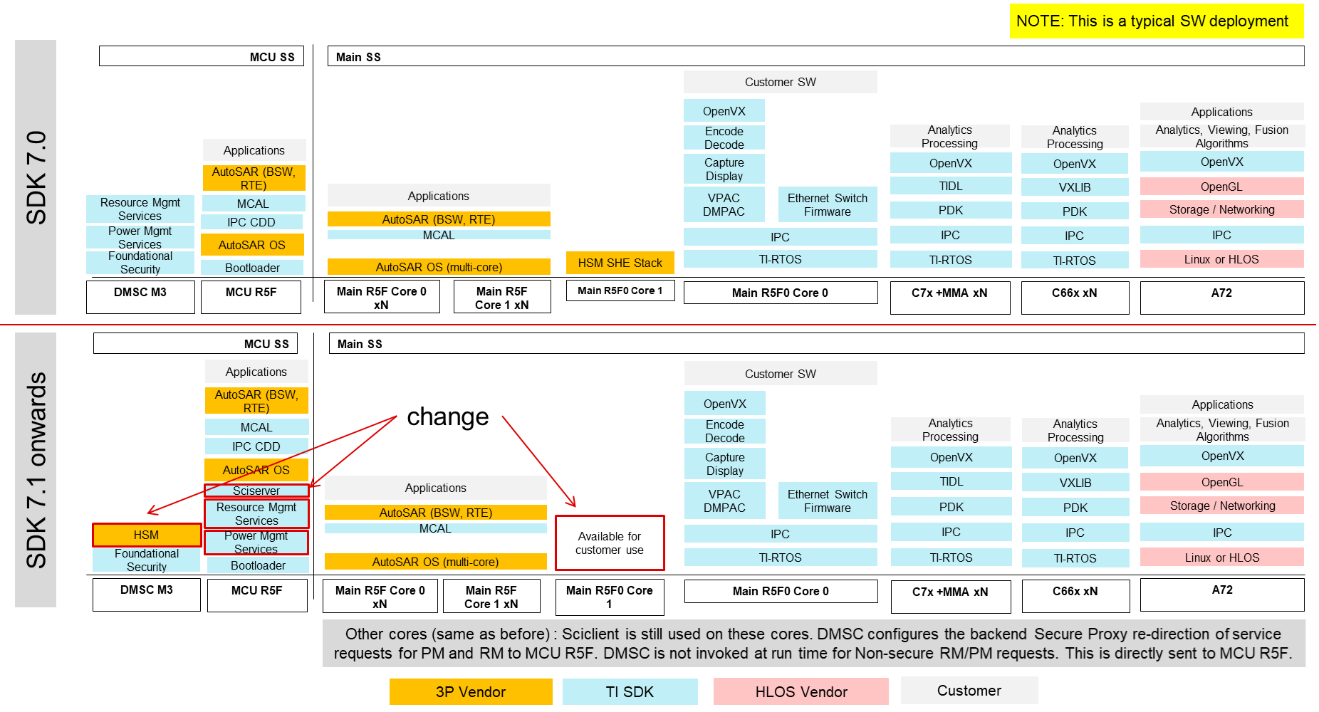
Purpose of DMSC firmware change
- Secure HSM functions can run on a DMSC Security Island
- Free a main domain R5F for general customer use.
- Enables MCU Only mode with HSM functions on DMSC
- Lockstep Safety R5F runs safety critical PM & RM functions.
sign secure boot
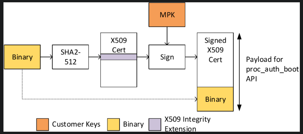
Signing an unencrypted binary for secure boot ^unecrypted
signing-pm-rm-and-core-board-configurations^1b50a0
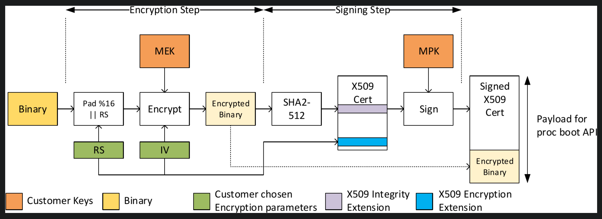
Signing an unencrypted binary for secure boot ^crypted
signing-security-board-configuration
signing-procedure-for-optimized-boot-time
1 | This sequence is only applicable to am65x, am65x_sr2, and j721e devices. This format is deprecated for all other devices which support the [combined boot image format](https://software-dl.ti.com/tisci/esd/22_01_02/3_boardcfg/BOARDCFG_COMBINED_IMG_FORMAT.html). |
Due to the asymmetric key verify operation when authenticating the signed board configuration, there is ~4 ms increase in boot time compared to using an unsigned board configuration. To reduce the boot time increase, System Firmware offers an alternative way of supplying signed board configuration. This approach has two key differences from the normal approach.
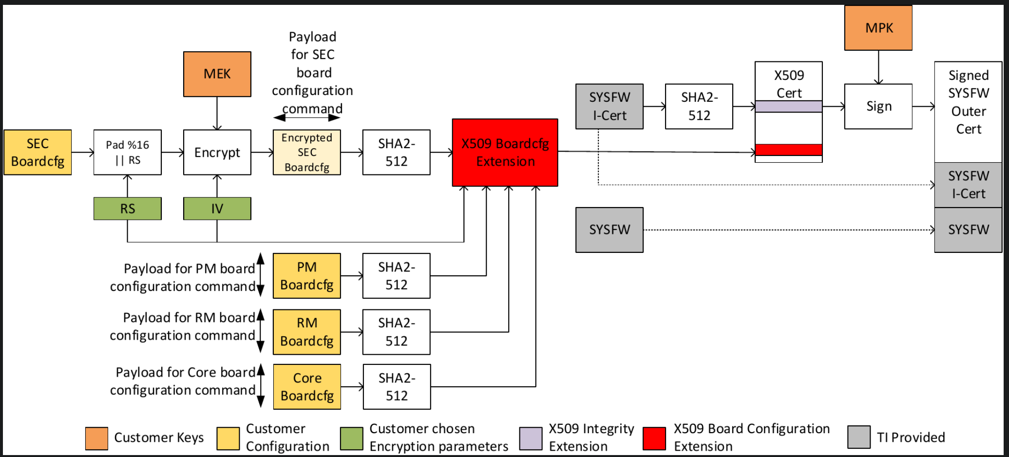
- Populate
pmBoardCfgHash,rmBoardCfgHashandboardCfgHashwith the SHA2-512 hashes of PM Board configuration, RM board configuration and the core board configuration blobs respectively.Device Type Boardcfg signing required Signing approach TISCI message payload Boardcfg extension in SYSFW Outer Certificate GP No NA Raw boardcfg NA HS Yes Development Signed certificate + encrypted boardcfg Do not include HS Yes Boot time optimized encrypted boardcfg Include Device Type Boardcfg signing required Signing approach TISCI message payload Boardcfg extension in SYSFW Outer Certificate GP No NA Raw boardcfg NA HS Yes Development Signed certificate + raw boardcfg Do not include HS Yes Boot time optimized raw boardcfg Include
KEK and DKEY
Using Derived KEK on HS devices — TISCI User Guide
- KEK is a randomly generated symmetric key
- KEK is made using NIST certified tester routine
KEK is different for each deviceand is not correlated in any ways with keys issued on others devices.- KEK is not stored in any database or retained in any manufacturing tester
- KEK is burnt in TI factory.
1 | KEK以硬件形式被送入DMSC内部的AES引擎。携带KEK的电子引信被标记为读和写保护。因此,KEK只能通过DMSC的AES引擎访问。每个设备的KEK都是不同的 |
密钥推导方法 key-derivation-method
1 | DKEK的计算在每个设备上都是确定性的。对于一个给定的主机、标签和上下文,即使在同一设备上重启,导出的KEK也是一样的。 |
Derived KEK TISCI Description — TISCI User Guide
tisci-msg-sa2ul-set-dkek-set-dkek
tisci-msg-sa2ul-release-dkek-release-dkek erase key
tisci-msg-sa2ul-get-dkek-get-dkek
如何使用DKEK (了解)
Comparing the two approaches
| Option 1 | Option 2 |
|---|---|
| DKEK programmed directly into SA2UL DKEK registers. | DKEK is provided to host as a response to a TISCI message. |
| No separate firewalling is required for DKEK. | Host must firewall memory where it is storing DKEK. |
DKEK can only be used through SA2UL. Host must set the USE_DKEK
flag to true in the SA2UL security context. Key must not be populated
in the SA2UL security context. |
DKEK can be used in two ways
|
| Only one host can use this approach at a time. There is only one set of SA2UL DKEK registers. Access to these registers for encryption/decryption is controlled by DKEK privid register. System Firmware programs the DKEK privid register with the privid of the host who has invoked the TISCI_MSG_SA2UL_SET_DKEK API. Only this host can use DKEK via the SA2UL DKEK registers until DKEK is released via TISCI_MSG_SA2UL_RELEASE_DKEK | Multiple hosts can use DKEK at the same time using this approach. Each host manages its own DKEK. |
| TISCI_MSG_SA2UL_SET_DKEK and TISCI_MSG_SA2UL_RELEASE_DKEK API are used in this approach. | TISCI_MSG_SA2UL_GET_DKEK is used in this approach. |
We recommend using Approach 1 wherever possible to maintain the secrecy of DKEK.
OTP
Using Extended OTP on HS devices — TISCI User Guide
K3 family of devices have a set of one-time programmable(OTP) efuses to carry root of trust keys and other information used during device boot. The purpose of these efuses is fixed. K3 family of devices have another set of OTP efuses for general purpose use by the customer. We refer to these efuses as extended OTP. In this document, we describe how the extended OTP can be accessed through TISCI API. This document must be read along side
1 | 两套OTP: |
The hardware allows each individual OTP row (not MMR) to be locked to prevent modification. Once the OTP row is locked, any bit in the row can never be modified.
keyWriter
high-security-hs-device-sub-types
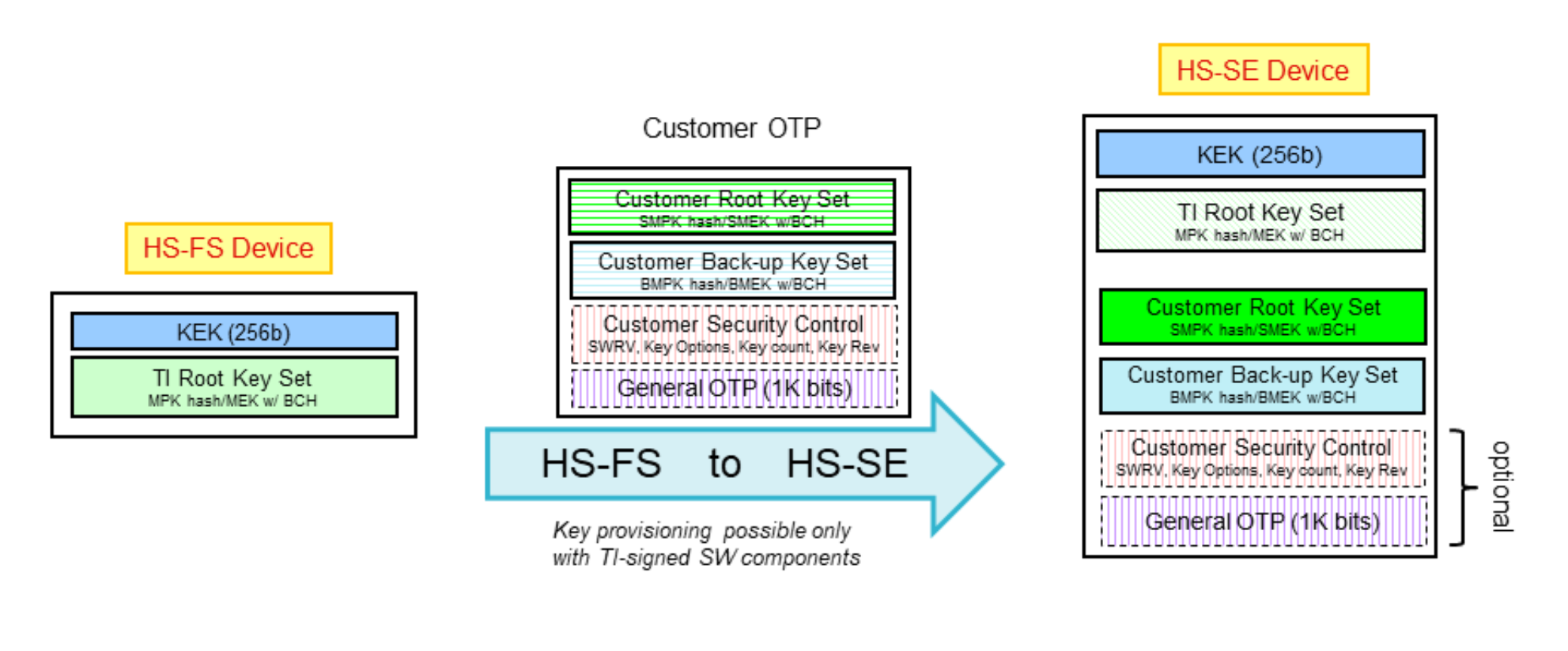
HS-FS (High Security - Field Securable): Device type before customer keys are programmed (the state in which the device leaves TI factory). In this state, device protects the ROM code, TI keys and certain security peripherals. HS-FS devices do not enforce secure boot process.
System Firmware binary is signed by the TI Private key (TI MPK) [[#^1b50a0]]
HS-SE (High Security – Security Enforced): Device type after customer keys are programmed. HS-SE devices enforce secure boot.
- System Firmware binary is encrypted by the TI Encryption key (TI MEK), and signed by the TI Private key (TI MPK).
Customer has to dual sign it with their private key (SMPK/BMPK). (Refer Signing an encrypted binary for secure boot)
In order to convert a HS-FS device to HS-SE device, one has to program the customer root key set (optionally backup key set) on the target device, using OTP Keywriter.
The following figure illustrates the procedure to be followed to generate the required x509 certifcate for key writing.
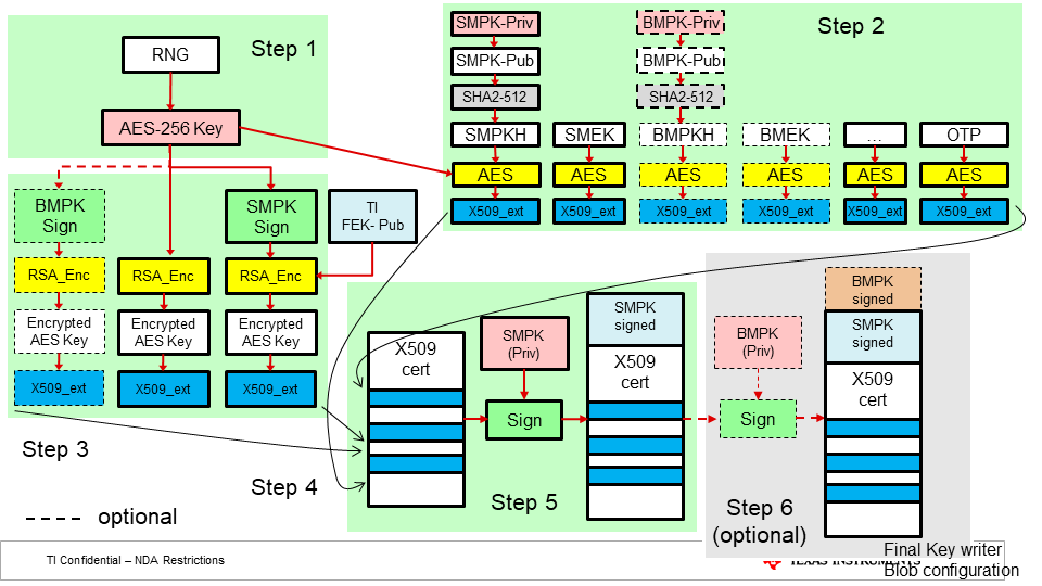
| Key | Description | Notes |
|---|---|---|
| BMEK | Backup Manufacturer Encryption Key | 256-bit Customer encryption key for encrypted boot |
| BMPKH | Backup Manufacturer Public Key Hash | BMPK is 4096-bit customer RSA signing key |
| EXTENDED OTP | Extended OTP array | 1024 bit extended otp array |
| KEYCNT | Key count | 2 if BMPK, SMPK are used, 1 if SMPK is used, 0 if none |
| KEYREV | Key revision | Can have a maximum value = key count |
| MEK Options | SMEK/BMEK options | (Reserved for future use) 5 bit value |
| MPK Options | SMPK/BMPK options | (Reserved for future use) 10 bit value (split into 2 parts) |
| MSV | Model specific value | 20 bit value with 12 bit BCH code |
| SMEK | Secondary Manufacturer Encryption Key | 256-bit Customer encryption key for encrypted boot |
| SMPKH | Secondary Manufacturer Public Key Hash | SMPK is 4096-bit customer RSA signing key |
| SWREV-BOARDCONFIG | Secure Board Configuration software revision | 128 bit value (64 without double redundancy) |
| SWREV-SBL | SBL software revision | 96 bit value (48 without double redundancy) |
| SWREV-SYSFW | Firmware software revision | 96 bit value (48 without double redundancy) |
SMPK (Secondary Manufacturer Public Key) ^7ad323
BMPK ( Backup Manufacturer Public Key) ^edb701